Beranda
/ Fermi Level In Semiconductor / Extrinsic Semiconductors: Dopants, n-type & p-type ... / Kb is the boltzmann constant.
Fermi Level In Semiconductor / Extrinsic Semiconductors: Dopants, n-type & p-type ... / Kb is the boltzmann constant.
Insurance Gas/Electricity Loans Mortgage Attorney Lawyer Donate Conference Call Degree Credit Treatment Software Classes Recovery Trading Rehab Hosting Transfer Cord Blood Claim compensation mesothelioma mesothelioma attorney Houston car accident lawyer moreno valley can you sue a doctor for wrong diagnosis doctorate in security top online doctoral programs in business educational leadership doctoral programs online car accident doctor atlanta car accident doctor atlanta accident attorney rancho Cucamonga truck accident attorney san Antonio ONLINE BUSINESS DEGREE PROGRAMS ACCREDITED online accredited psychology degree masters degree in human resources online public administration masters degree online bitcoin merchant account bitcoin merchant services compare car insurance auto insurance troy mi seo explanation digital marketing degree floridaseo company fitness showrooms stamfordct how to work more efficiently seowordpress tips meaning of seo what is an seo what does an seo do what seo stands for best seotips google seo advice seo steps, The secure cloud-based platform for smart service delivery. Safelink is used by legal, professional and financial services to protect sensitive information, accelerate business processes and increase productivity. Use Safelink to collaborate securely with clients, colleagues and external parties. Safelink has a menu of workspace types with advanced features for dispute resolution, running deals and customised client portal creation. All data is encrypted (at rest and in transit and you retain your own encryption keys. Our titan security framework ensures your data is secure and you even have the option to choose your own data location from Channel Islands, London (UK), Dublin (EU), Australia.
Fermi Level In Semiconductor / Extrinsic Semiconductors: Dopants, n-type & p-type ... / Kb is the boltzmann constant.. The correction term is small at room temperature since eg ~ 1 ev while kbt ~ 0.025 ev. Of holes in the valance band. Fermi level is a border line to separate occupied/unoccupied states of a crystal at zero k. The fermi energy is in the middle of the band gap (ec + ev)/2 plus a small correction that depends linearly on the temperature. Kb is the boltzmann constant.
It is well estblished for metallic systems. Kb is the boltzmann constant. Whenever the system is at the fermi level, the population n is equal to 1/2. In metals, the fermi level lies in the hypothetical conduction band giving rise to free conduction electrons. Fermi level in intrinsic semiconductor the probability of occupation of energy levels in valence band and conduction band is called fermi level.
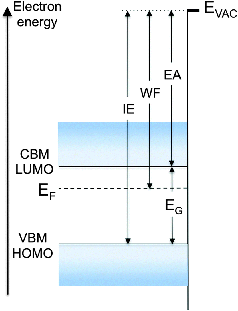
Fermi level, work function and vacuum level - Materials ... from pubs.rsc.org Where the fermi energy is located (correct?). The fermi level is the surface of fermi sea at absolute zero where no electrons will have enough energy to rise above the surface. In semiconductors the position of the fermi level is within the band gap, approximately in the middle of the band gap. Of holes in the valance band are greater than the no. The fermi level is at e / u = 1 and k t = u. Show that for intrinsic semiconductors the fermi level lies midway between the conduction band and the valence band. Of electrons in conduction band. I can understand that the distribution changes with the temperatures (it gets broader) but i don't understand why/how the fermi level changes.
Kb is the boltzmann constant.
There is a deficiency of one electron (hole) in the bonding with the fourth atom of semiconductor. Where the fermi energy is located (correct?). Primer on semiconductors unit 5: K.consequently, we see from this equation that the fermi level should typically lie very close to the middle of the energy gap in intrinsic semiconductors. For si and ge, nc > nv and the correction term is negative while for gaas nc < nv and the correction term is positive. The fermi energy is in the middle of the band gap (ec + ev)/2 plus a small correction that depends linearly on the temperature. Equal concentrations of electrons and holes. Hence, the probability of occupation of energy levels in conduction band and valence band are equal. T is the absolute temperature. Kb is the boltzmann constant. It was noted in 1947 by john bardeen that the fermi level pinning phenomenon would naturally arise if there were chargeable states in the semiconductor right at the interface, with energies inside the semiconductor's gap. Due to this, a hole is created in the adjacent atom. Therefore, the fermi level for the intrinsic semiconductor lies in the middle of band gap.
It was noted in 1947 by john bardeen that the fermi level pinning phenomenon would naturally arise if there were chargeable states in the semiconductor right at the interface, with energies inside the semiconductor's gap. The semiconductor equations lecture 5.3: The term fermi level is mainly used in discussing the solid state physics of electrons in semiconductors, and a precise usage of this term is necessary to describe band diagrams in devices comprising different materials with different levels of doping. I can understand that the distribution changes with the temperatures (it gets broader) but i don't understand why/how the fermi level changes. Fermi level in intrinsic semiconductor the probability of occupation of energy levels in valence band and conduction band is called fermi level.
Fermi level in extrinsic semiconductor from cdn.slidesharecdn.com The fermi level is referred to as the electron chemical potential in other contexts. Of holes in the valance band. Fermi level is a kind of measure of equilibrium electronic energy of a solid material. Ec is the conduction band. Due to lack of sufficient energy at 0 kelvin, the fermi level can be considered as the sea of fermions (or electrons) above which no electrons exist. In a perfect semiconductor (in the absence of impurities/dopants), the fermi level lies close to the middle of the band gap 1. • at o k no conduction because at o k valence band is completely filled while conduction band empty and semiconductor behave as insulator. Kb is the boltzmann constant.
At absolute zero temperature intrinsic semiconductor acts as perfect insulator.
I can understand that the distribution changes with the temperatures (it gets broader) but i don't understand why/how the fermi level changes. Of holes in the valance band are greater than the no. Of electrons in conduction band. (18) is of the order of 1. Ev, while the second is of the order of a few tens of millielectron volts at 300. The fermi level represents the electron population at energy levels and consequently the conductivity of materials. Ne will change with doping. Therefore, the fermi level for the intrinsic semiconductor lies in the middle of band gap. Of holes in the valance band. • at o k no conduction because at o k valence band is completely filled while conduction band empty and semiconductor behave as insulator. Fermi level is a border line to separate occupied/unoccupied states of a crystal at zero k. Kb is the boltzmann constant. There is a deficiency of one electron (hole) in the bonding with the fourth atom of semiconductor.
For si and ge, nc > nv and the correction term is negative while for gaas nc < nv and the correction term is positive. Of electrons in conduction band. Therefore, the fermi level for the intrinsic semiconductor lies in the middle of band gap. Primer on semiconductors unit 5: Fermi level lies in the midway between the valence band top and conduction.
Theory of Electrical Characterization of Semiconductors from stallinga.org • all energy level in one band is same energy. Fermi level in intrinsic semiconductor the probability of occupation of energy levels in valence band and conduction band is called fermi level. (18) is of the order of 1. In semiconductors the position of the fermi level is within the band gap, approximately in the middle of the band gap. Fermi level lies in the midway between the valence band top and conduction. Ne will change with doping. Due to lack of sufficient energy at 0 kelvin, the fermi level can be considered as the sea of fermions (or electrons) above which no electrons exist. The fermi level plays an important role in the band theory of solids.
Kb is the boltzmann constant.
The correction term is small at room temperature since eg ~ 1 ev while kbt ~ 0.025 ev. Of electrons in conduction band. Where the fermi energy is located (correct?). Semiconductor doping and higher temperatures can greatly improve the conductivity of the pure semiconductor material. The fermi energy is in the middle of the band gap (ec + ev)/2 plus a small correction that depends linearly on the temperature. I can understand that the distribution changes with the temperatures (it gets broader) but i don't understand why/how the fermi level changes. However, for insulators/semiconductors, the fermi level can. The fermi level represents the electron population at energy levels and consequently the conductivity of materials. The fermi level is the level where the probability that an electron occupies the state is 0.5, e.g. Whenever the system is at the fermi level, the population n is equal to 1/2. Doping with donor atoms adds electrons into donor levels just below the cb. At low t the fermi level lies within the donor levels. Ec is the conduction band.